Low-Temperature Sintering to Form Copper Electrodes
Oxidation-Resistant Nano Copper Powders

閉じる
閉じる
Search

As environmental pressures mount, efficient use of natural resources and achieving a sustainable society have become essential. As AI, IoT, and big data drive rapid advances in electronics and information technology, demand for electronic devices continues to grow. These devices depend on circuits formed on substrates, a process that consumes large amounts of energy and imposes a heavy environmental burden. In response, the industry is rethinking conventional production methods and pursuing technologies that are cleaner and more resource-efficient. Printed electronics is one such technology. It consumes less energy than conventional processes while yielding lightweight, flexible devices. Applied to substrates such as resin films, the technology is expected to gain wide adoption for its design freedom and low environmental impact. This article examines the potential of printed electronics and the metal-complex conductive pastes that Sumitomo Metal Mining is developing.
Printed electronics is a cutting-edge technology for fabricating electronic circuits and devices on both rigid and flexible substrates using conductive, semiconducting, and insulating inks. The dominant method today is photolithography, in which the entire substrate is coated and the unwanted areas are then etched away with chemicals to leave the circuit pattern. This process consumes large volumes of water for plating and produces chemical waste such as spent copper plating solutions and photoresist, thus having a significant environmental impact. Printed electronics, by contrast, forms circuits directly on the substrate, conserving resources and energy while reducing carbon emissions, weight, and cost. This technology has therefore drawn growing attention across a range of industries.

Advances in IT and the spread of IoT are bringing digital functionality to an expanding range of products. Consequently, electronic devices are becoming both more varied and more complex, from automobiles and smartphones to ultralight wearables and foldable displays, in industrial and consumer markets alike. Printed electronics offers high productivity and a wide choice of substrates, making it possible to produce thinner, lighter, and larger-area products at high speed and low cost. Since conductive ink is deposited only where circuit patterns are required, the technology substantially shortens the production process and reduces equipment investment as well as material and energy consumption.
Manufacturers use various printing methods, including inkjet and screen printing, to produce printed electronics. These methods allow manufacturers to print electronic inks and conductive materials directly onto substrates without water-intensive plating. This direct printing process is shorter than traditional manufacturing processes, delivering energy savings, greater flexibility, and improved production efficiency. Additionally, it lowers CO2 emissions and reduces water consumption.
What is Conductive Ink? Exploring its Applications and Cost-Effective Solutions
Because this process uses only the required amounts of conductive copper and insulating materials, manufacturers can avoid large-scale equipment and high-temperature processes. Consequently, printed electronics significantly reduces energy consumption and carbon dioxide emissions compared with traditional manufacturing.
Eliminating complex manufacturing processes reduces production times and costs. In the roll-to-roll method, the printing machine feeds rolled substrates through the mechanism and then re-rolls the substrates. This method allows manufacturers to mass-produce electronic circuits at a high speed. Consequently, this technology provides significant advantages over sheet-based methods.
Printed electronics makes it possible to print on flexible and large-area substrates, which were difficult to achieve with conventional methods. This on-demand manufacturing approach also supports the development of new products tailored to a wide variety of needs.
Manufacturers apply printed electronics technology in various fields, including displays, solar cells, RFID tags, and sensors. This technology is also suitable for low-volume production of a wide variety of custom products.

Printed electronics improves the manufacturing of thin, flexible displays. This technology allows manufacturers to produce bendable displays, transparent displays, and roll-up screens that were difficult to produce using conventional methods. These advancements enable new products, such as smartphones, advertising displays, and wearable devices like smartwatches.
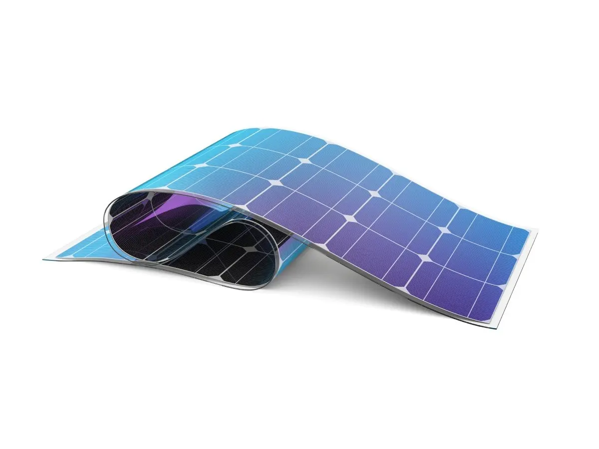
Printed electronics enables manufacturers to produce lightweight, flexible solar cells. Users can install these solar cells where traditional rigid panels cannot be used, such as on building roofs and walls, or on clothing and bags. Low-cost manufacturing also contributes to the expansion of renewable energy.
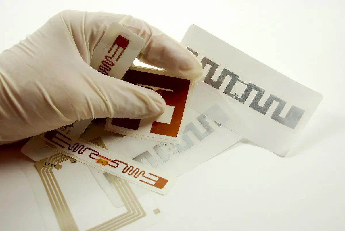
Since manufacturers can mass-produce RFID tags at a low cost, they can expand the use of these tags for tracking logistics, managing inventory, and identifying individual items. Additionally, printing on flexible materials allows manufacturers to apply RFID tags to clothing, books, and food packaging. Until now, these applications have been difficult to achieve with traditional RFID tags.
Sensors are essential to a "smart" society. Many industries require these sensors, including energy, healthcare, autonomous driving, smart factories, and smart textiles. To build advanced sensor systems, manufacturers require inexpensive devices that are powerful and highly adaptable, while being small and lightweight. Printed electronics is a technology that meets these requirements.
Printed electronics technology is suitable for low-volume production of a wide variety of products. This technology allows manufacturers to produce custom electronic circuits easily and cost-effectively, even in small production lots, supporting the development of products tailored to specific needs, such as sensor networks, displays for specialized applications, and individual wearable devices.
Sumitomo Metal Mining is developing a copper-powder-based Metal Organic Decomposition (MOD) paste. This material provides high conductivity and high stability. This paste enables thick-film formation, which was difficult to achieve with conventional conductive materials. Thick-film formation allows manufacturers to form low-resistance, high-performance electronic circuits that can carry high electrical currents on flexible substrates. Industry experts classify this paste as an environmentally friendly material, since thick-film formation also enables large-area applications such as solar panels and large displays.
MOD Paste (Metal Organic Decomposition)

The evolution of printed electronics technology is transforming how electronic devices are manufactured while enabling new product development. With its environmental and economic benefits, this technology is expected to play a key role in building a sustainable society.
Printed electronics is an innovative technology expected to find applications in various industrial fields, offering flexibility, cost efficiency, and low environmental impact. Sumitomo Metal Mining is developing a copper-powder-based MOD Paste, which is an effective material for printed electronics and is suitable for flexible substrates.
X-Mining combines profound expertise in materials science with industry insights to innovate and solve challenges. If you see potential for collaboration, please contact us with any questions.
Introducing Sumitomo Metal Mining’s material products,
which are the starting point for X-MINING innovation.