Article

閉じる
閉じる
Search

Higher density
Step structures and embedded components enable thin, high-density mounting.

Fine processing
Creates high-precision free-form shapes and micro-holes through blasting.

High reliability
Designed with thermal management considerations to ensure stability and dependability for long-term use.
Design flexibility
Enables advanced functionality and complex device configurations by using cavity structures (steps) and blasting processes.
High-density printed circuit boards combine structural design with machining technologies to support the miniaturization and extended functionality of electronic devices. By combining step and recessed structures with processing of micro-holes and narrow slots, they enable highly functional designs in limited spaces. They also enable high-density mounting and precision structures, even on conventional flat boards, and enhances freedom of design for next-generation devices.
This page introduces (1) the cavity structure that lowers mounting height with step and recess designs, and (2) thin-board blasting process that handles free-form shapes, micro holes, and narrow slits.
A cavity board is a printed circuit board with recesses (cavities) formed in the board, allowing electronic components to be placed within the board. By using the steps, it can achieve miniaturization, a lower profile, higher density, and better heat dissipation. It can also reduce resin-molded parts and streamline assembly, making it an effective technology for electronic devices and module boards that require minimization.
Below are some examples of how cavity structures have provided solutions to solve design challenges that were difficult to address with conventional boards.
By adopting a cavity structure, module boards can be made thinner and lower profile, helping to miniaturize the final product. It also shortens the distance between components, giving designers more freedom.
By forming recess (cavities) in the board and mounting electronic components there, the module can be downsized and minimalized.
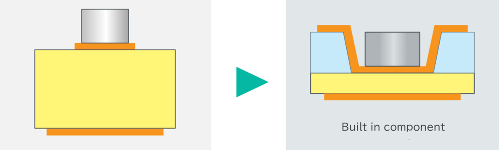
Using cavity structures makes it easier to place components in limited space, supporting high-density mounting.
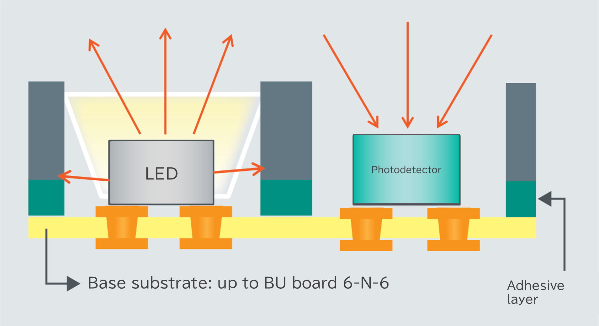
By using the cavity walls, the resin-molded parts needed for module assembly can be reduced. This helps streamline the resin parts, reduce molding, and reduce time, contributing to more efficient assembly.
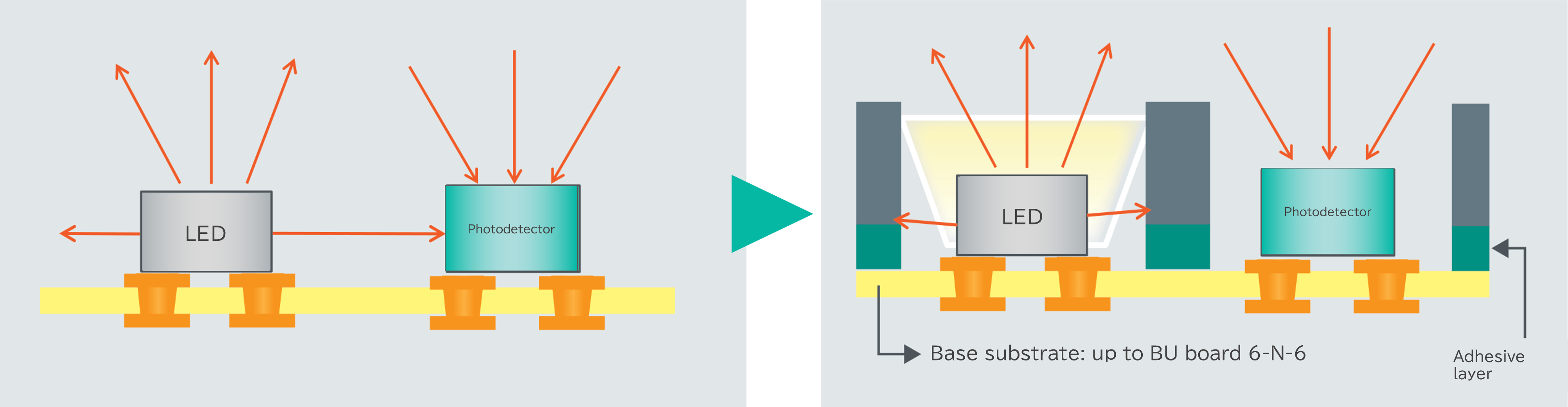
Cavity boards can be applied as follows.
| Application | Details |
|---|---|
| RF modules | Improves high-frequency characteristics through shorter wiring, module downsizing and minimalization, and enhanced shielding performance. |
| MEMS sensors | Protects sensing elements, secures sensing space, and optimizes the sealing structure. |
| Power devices | Provides space for mounting large chips, improves design flexibility, and enhances heat dissipation and mounting reliability. |
| Optical devices | Smaller, lower-profile modules with space for optical paths and alignment. |
Semi-Flex PCB
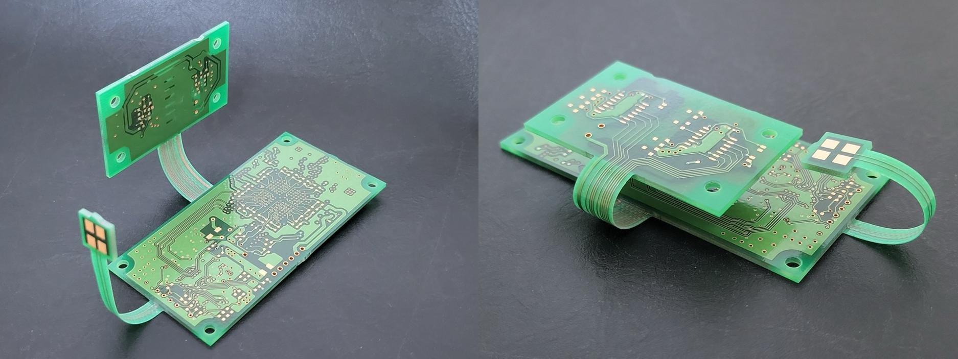
A printed circuit board, in which part of a conventional rigid board is thinned enough to be bent, can be used in applications that do not require repeated flexing like a rigid-flex board, and enables 180-degree bending without connectors or cables.
*You will be redirected to Shinko Co., Ltd.'s website in Japanese.
High-density mounting requires technology capable of processing intricate shapes with high precision. With significant design flexibility, *this technology handles a wide range of designs, from free-form shapes like elliptical holes and contour following shapes, to small diameter holes and narrow slits. The ability to process multiple holes simultaneously also contributes to production efficiency. Shinko has adapted blasting technology for PCB manufacturing, enabling the mass production of holes and slits.
The following are examples of how blasting process technology has played a part in solving design challenges that were difficult to address with conventional boards.
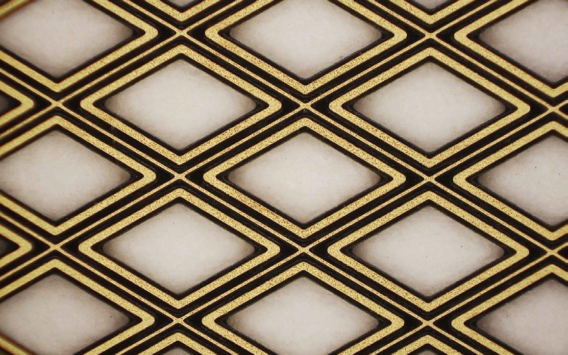
Conventional processing faced challenges with dimensional accuracy and shape reproduction in boards that require fine structures. Blasting process achieves both precision and fine detail with excellent dimensional accuracy, leading to higher density, processing quality improvement, and reliability.
Able to process holes in a wide variety of shapes, including contour-following shapes and elliptical holes.
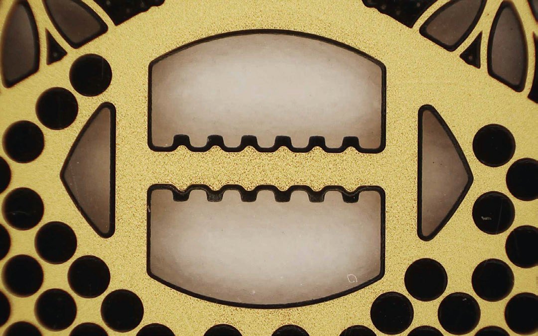
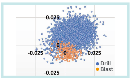
By achieving a hole position accuracy of ±0.025 mm, it contributes to improved positional accuracy for resin molding and mounted components.
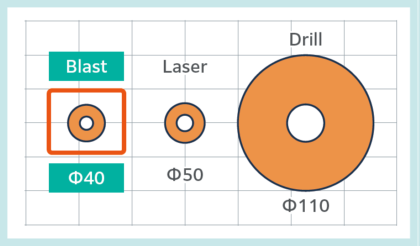
Can form vias as small as φ40 μm. With an aspect ratio of 1, vias of φ40 μm are possible at t40 μm.
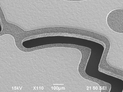
Using blasting process, narrow slits can be reduced to 0.1 mm wide under an aspect ratio of 1. This supports miniaturization and high-density design through micro-scale openings.
Masks allow the required holes to be formed simultaneously, eliminating the need to process one hole at a time as with drilling or laser methods thus significantly improving processing efficiency.

| Applications | Details |
|---|---|
| Blasting Processes | Supports micro openings, narrow slits, and special shapes, with batch processing using a mask instead of one hole at a time. |
| Inductor Substrates (oval holes, etc.) |
Supports processing of inductor boards that require shape flexibility, such as oval holes and special openings. |
| Wearables (conforming to housing contours) |
Capable of processing curved surfaces and complex housing shapes, making it suitable for exterior components of small, thin devices. |
| Healthcare / Sensors (special shapes and precision processing) |
Suitable for sensor components and healthcare devices that require fine openings and special shapes. |
*You will be redirected to Shinko Co., Ltd.'s website in Japanese.
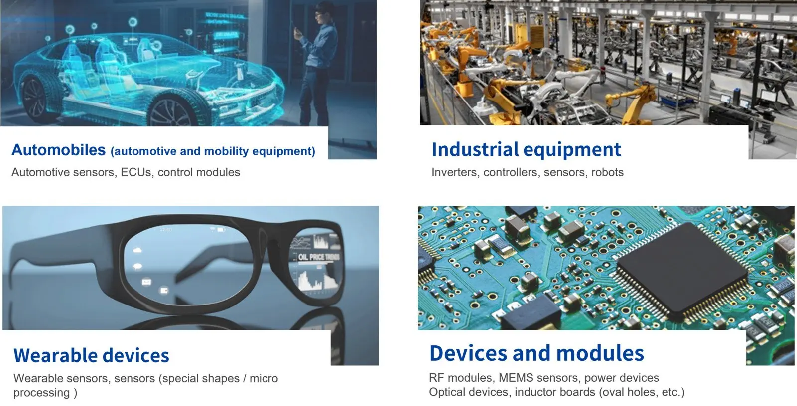
Used in electronic devices that require miniaturization, such as portable high-performance devices, module boards, and high frequency communication equipment. Below are examples of high grade products.
X-Mining combines deep materials science expertise with industry insights to innovate and solve challenges.
If you see potential for collaboration, please contact us with any questions.
Introducing Sumitomo Metal Mining’s material products,
which are the starting point for X-MINING innovation.