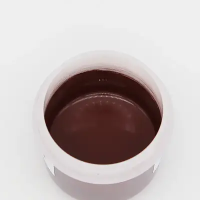
Nano Copper Powder with Good Oxidation-resistant
Powders
【R&D】

閉じる
閉じる
Search
The performance and multifunctionality of all electronic devices—smartphones, optical communication devices, other IoT devices, electric vehicles (EVs), and medical devices—continue to advance with each passing day. While these technological advances make everyday life more convenient, they also present new challenges for engineers engaged in product development. It seems that many developers are struggling as it has become difficult to find optimal solutions based on a single technology or material.
What is needed today is a completely new option that integrates materials and technologies at the highest levels. Sumitomo Metal Mining, a manufacturer that develops conductive materials and other materials, and Shinko, a manufacturer of unique printed circuit boards (PCBs) based on proprietary technologies, have launched a co-creation initiative to provide new products that meet a diverse range of needs. They are currently developing innovative PCBs that offer high added value never seen before.
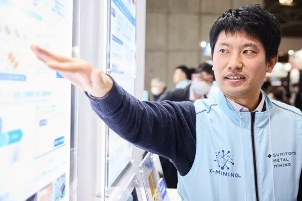
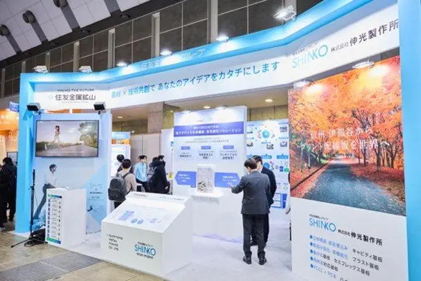
One such effort was showcased at the 40th edition of NEPCON JAPAN, held at Tokyo Big Sight from January 21 to 23, 2026. We will explore the current status and future potential of co-creation, while looking back on the day of the show, when people involved in development at various manufacturers stopped by the booth and showed strong interest.
NEPCON JAPAN is a large-scale technology show for electronic components, semiconductors, power devices, and other electronics technologies. As one of Asia’s largest electronics technology shows and a venue where world-leading technologies converge, it attracts engineers involved in product development from various manufacturers, who come to the show in search of inspiration for new ideas or new technological options for their development.
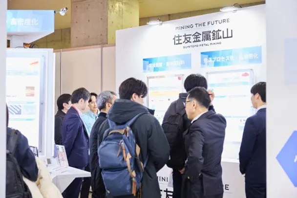
Held at Tokyo Big Sight from January 21 to 23, 2026, the 40th edition of NEPCON JAPAN was attended by some 78,000 visitors over the three days of the event (based on preliminary assessment). The joint exhibition booth hosted by Sumitomo Metal Mining and Shinko drew a constant stream of people who expressed significant interest in the products.
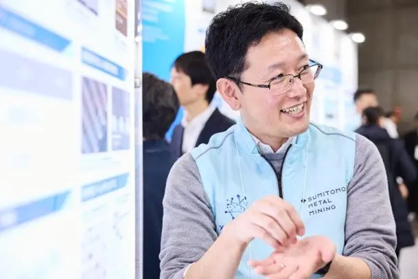
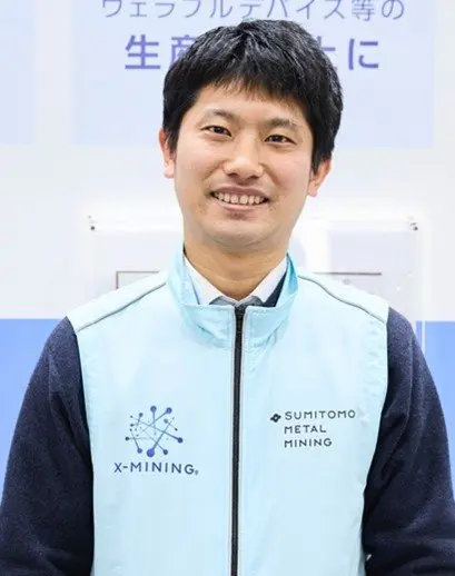
“The demand for high-performance semiconductors, electronic devices, and other technologies needed to enrich people’s lives is growing daily. But while these technologies are rapidly advancing, the supply of the materials needed to achieve real-world application of the technologies is failing to keep up. I think this is a challenge facing many manufacturers involved in developing power semiconductors, optical devices, EVs, IoT devices, and medical devices,” says Kentaro Nakatsuji (Innovation Strategy Dept., Advanced Materials Div.), the Electronics Team Leader at Sumitomo Metal Mining. Nakatsuji is currently exploring the potential of conductive materials such as silver and copper that conduct electricity and bring next-generation technologies in the field to life.
According to Nakatsuji, “Silver has long been the metal of choice for its superior conductivity. But the price has reached historic highs due to factors such as the growing demand for electronic devices and the recent instability in the global situation. So, copper is drawing growing interest as an alternative. Copper is less expensive than silver and delivers high performance and ease of handling. There’s growing demand for next-generation conductive materials made from copper.”
Another factor driving the demand for new conductive materials is the dramatic evolution of electronic devices. As Nakatsuji points out, conventional materials no longer fully meet the performance requirements and specifications demanded by the market due to the never-ending trend toward higher power output, smaller and thinner designs, and enhanced multifunctionality.
“For example, when we incorporate high-power-consumption chips like AI semiconductors along with smaller high-density components, the high heat generation poses major challenges for board design,” explains Nakatsuji. “As the higher heat generation can negatively impact both the reliability and the performance of the chip, it’s critical to find a solution to handle the high electrical current required to power the chips via the board while meeting heat dissipation requirements. To solve this problem, it wasn’t enough simply to develop new conductive materials. We decided that we had to create an innovative board by combining the material with advanced processing technologies and to demonstrate to the market how our new material could offer new value by presenting actual products.”
To this end, Sumitomo Metal Mining launched a co-creation initiative with Shinko, a group company that manufactures PCBs. The initiative sought to develop a completely new type of PCB combining next-generation conductive materials developed by Sumitomo Metal Mining with Shinko’s superior precision processing technologies.
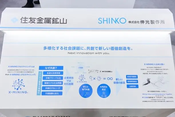
At their joint exhibition booth at this year’s NEPCON JAPAN, they showcased their co-creation efforts under the theme of “Solutions for Multifunctional, High-Performance Electronic Devices Realized Through Co-Creation Efforts Involving Materials and Technologies.” They introduced their newest materials and processing technologies that hold the potential to resolve development challenges across a broad range of fields.
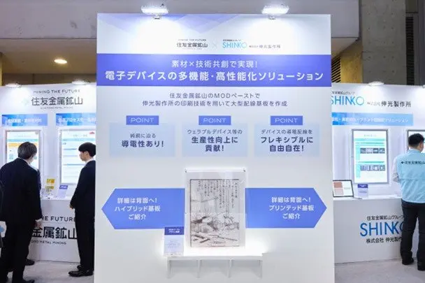
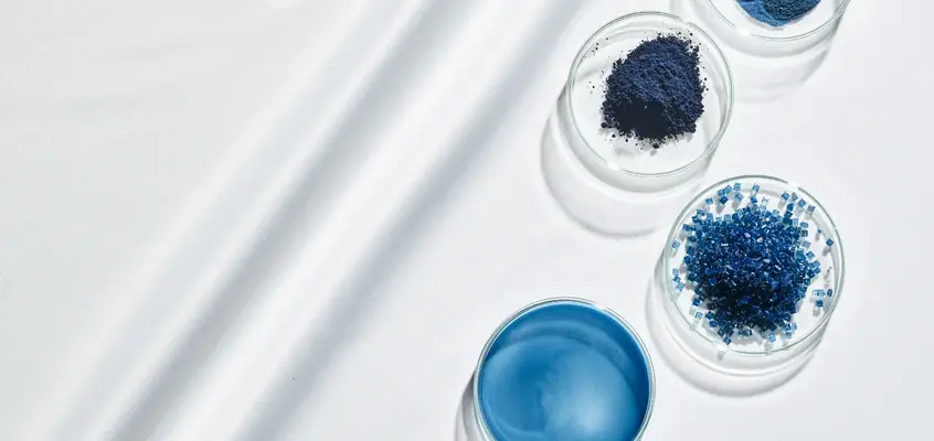
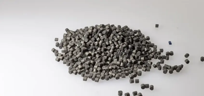
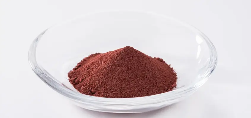
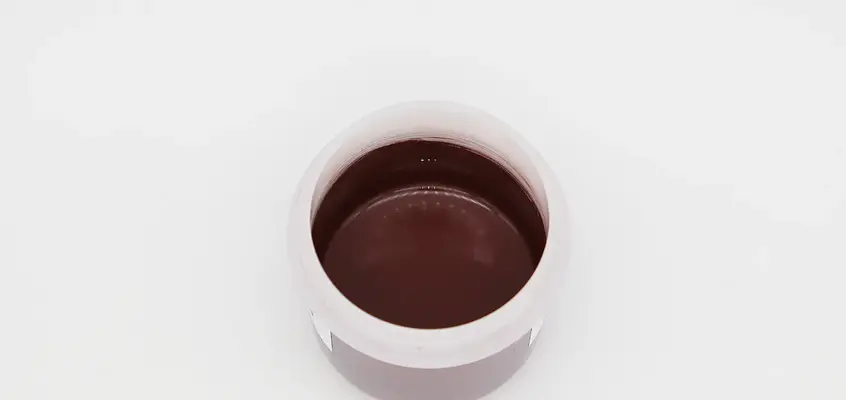
At the section showcasing their latest materials, they introduced the next-generation conductive materials, such as the oxidation-resistant nano copper powder, metal organic decomposition (MOD) paste, and flexible copper clad laminate (FCCL) developed by Sumitomo Metal Mining. Many people involved in development at various companies, who are seeking new alternatives to silver that is becoming increasingly costly, stopped by their booth to take a closer look.
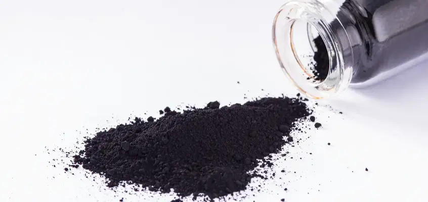
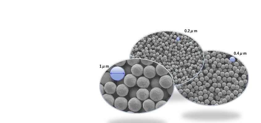
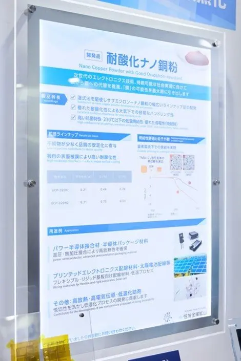
Oxidation-resistant nano copper powder is an extremely fine copper powder with particle sizes of 100 nm or 200 nm. It is expected to be used as a material for bonding semiconductor chips to their substrates and as a conductive material on resin substrates.
“Reducing copper powder particles to the nanoscale level makes it possible to sinter the powder at lower temperatures, around 200 °C,” says Nakatsuji. “This makes it possible to achieve higher performance in conventional applications where solder and other materials have been used as bonding materials, while keeping the same process. Although copper is much more susceptible to oxidation than silver, Sumitomo Metal Mining is taking full advantage of our long-established metal powder synthesis technologies to achieve high oxidation resistance, even with such fine powders. We overcame the disadvantages of copper while unlocking copper’s potential.”
MOD paste, a product developed using this copper powder, is a new conductive material for printed electronics* that combines copper powder with a metal complex ink.
*Printed electronics: Technology for forming electronic circuits by printing metal films (applying conductive ink/paste) only where needed
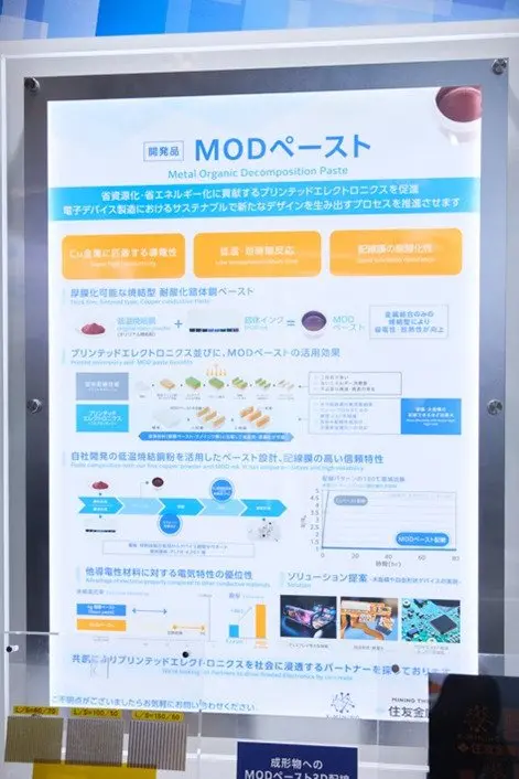
According to Nakatsuji, “Our MOD paste features high conductivity compared to conventional pastes made using resins and other materials. Applying this material by printing should make it possible to create serpentine electronic circuits and form wiring on 3D-molded objects. We anticipate a broad range of applications, including wearable devices and sensor devices.”
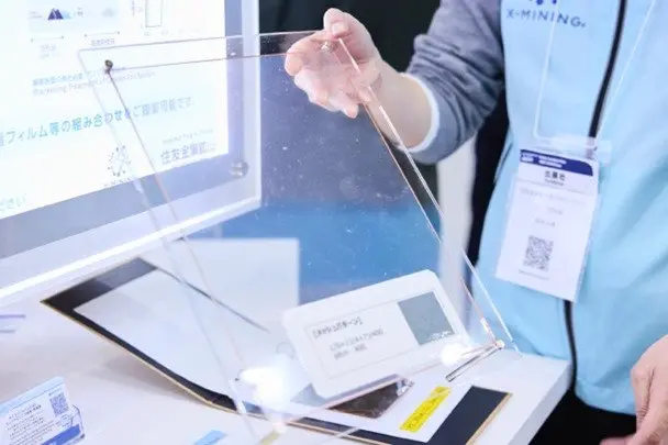
Sumitomo Metal Mining’s FCCL is a flexible substrate material consisting of copper laminated onto an organic resin film. One of its key features is an exceptionally smooth interface, with far fewer surface irregularities than conventional materials in the industry. It is also thin and uniform. Another notable feature is that it enables fine wiring.
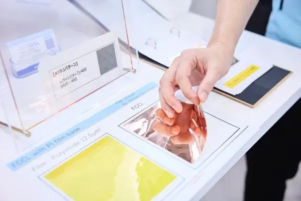
“The biggest advantage of using the new FCCL is that it allows the formation of extremely narrow and fine wiring, enabling the development of smaller, thinner products,” says Hiroki Matsui, a member of the development team (the Package Group, Product Development Dept., Advanced Materials Div.). “It’s also remarkably compatible with transparent resin films. Its high transparency makes it nearly impossible to see the copper lamination. That makes it suitable for use as a heater on automobile windshields.”
Since customers can choose a wide variety of resin films that meet their development needs, this product can open up new applications, which would previously have been hard to imagine, depending on the application idea.
“We’ve heard surprised reactions from visitors, such as, ‘I didn’t know something like this existed!’,” says Matsui. “I don’t think our job ends when we hand over materials. We want to discover new applications through co-creation efforts undertaken with our customers. Based on the results of these co-creation efforts, we’d like to design FCCL products with the properties our customers require.”
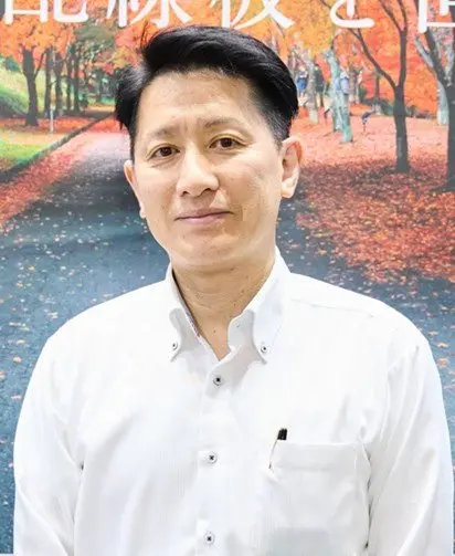
Shinko has proprietary processing technologies for high-precision, high-density PCBs, meaning it is ideally positioned to make the most of these new materials from Sumitomo Metal Mining.
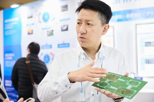
“When they hear the term ‘PCBs,’ I think most people imagine a flat green board with conductive wiring patterns on it,” says Yoshikazu Takagi (Chief of Sales Section 3, Sales Dept.) of Shinko. “Beyond such standard printed circuit boards (PCBs), Shinko manufactures unique PCBs that rely on proprietary processing technologies.”
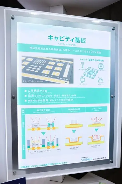
Shinko is a company dedicated to developing products like cavity substrates and semi-flex PCBs, which address various issues associated with electronic device manufacturing.
<
“A cavity refers to a hole or indentation,” explains Takagi. Cavity substrates are PCBs with a three-dimensional structure. With conventional flat boards, adjacent components can interfere with each other and generate noise. In contrast, cavity substrates have tiered surfaces that serve as shields between the components to prevent interference, which in turn makes it possible to position many components in close proximity and to build smaller products with higher density.”
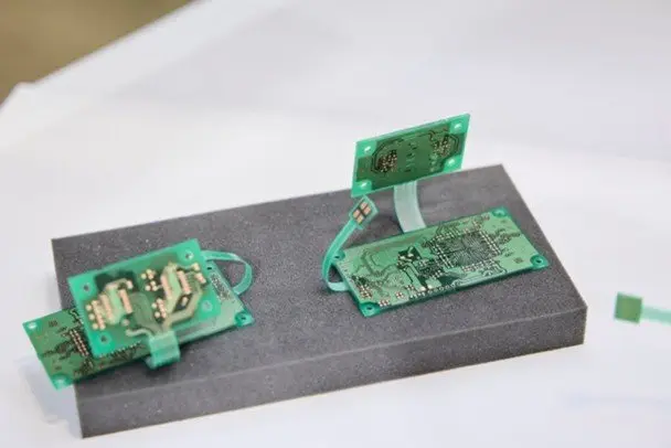
He continues, “Semi-flex PCBs are even more unique. They allow significant design flexibility by making a section of the board thin so that the section can be bent. Since they allow complex layouts without connectors or wiring cables, semi-flex PCBs reduce the number of molding and assembly processes while minimizing the number of required components and lowering costs.”
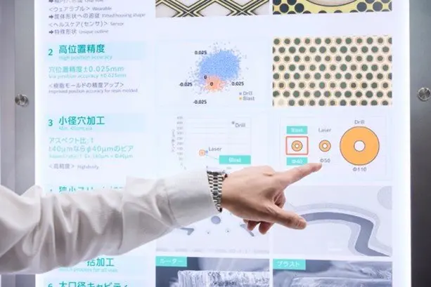
Another example illustrating Shinko’s advanced technological capabilities is its thin blast-processed substrate. Shinko applies a proprietary blast-processing technology to achieve ultra-fine processing that exceeds the limitations of conventional drilling, laser cutting, and routing technologies.
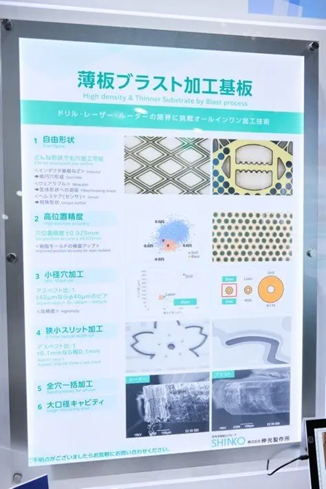
According to Takagi, “We drill holes in PCBs to allow electricity to pass through. With conventional laser processing, a hole with a diameter of 50 μm is generally considered to be the limit. Shinko’s blast-processing technology is capable of drilling holes as small as 40 μm, so small not even a single strand of hair can pass through them. Smaller holes make it possible to reduce the surface area of PCBs, which enables more compact products, and higher density will lead to improved performance.”
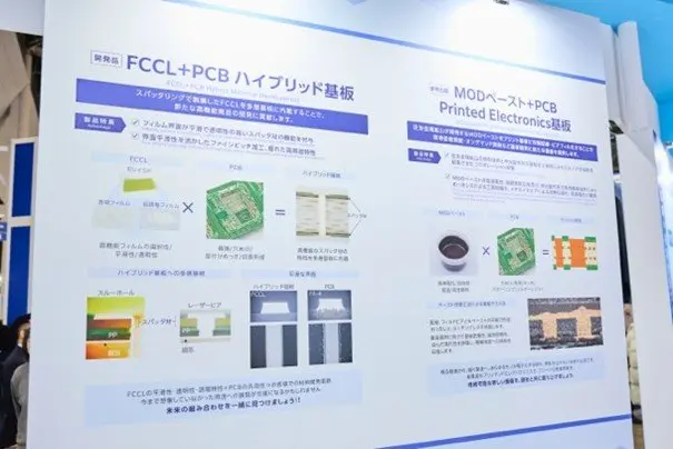
At the joint exhibition, examples of products that combine Sumitomo Metal Mining’s FCCL and MOD paste with Shinko’s PCBs were presented. While the technologies are still under development, they hold the potential to revolutionize the future of manufacturing.
“Materials manufacturers like Sumitomo Metal Mining often feel that there’s a divide between the company and end users,” says Nakatsuji. “Until now, it’s been hard for us to get a clear picture of how the materials we supply are ultimately used in the products of our customers. As the challenges posed by manufacturing grow more complex and sophisticated, a mere material is no longer sufficient to solve them. To create new solutions to such challenges, it’s essential to take an approach that involves developing technologies while incorporating feedback from partners who have different expertise.”
The goal of co-creation is to bring out each party’s strengths to generate greater value than what could have been achieved individually. Take, for example, the hybrid PCBs produced by combining FCCL and cavity substrates. Incorporating high-performance FCCL (sputter material) into the multilayered substrate enables the development of new high-performance products.
PCBs using MOD paste enable flexible wiring, contributing to the development of high-value-added products. The technology also reduces environmental impact by making more efficient use of raw materials. Both types of PCBs offer high added value achievable only through a co-creation approach. They represent a fusion of materials and processing technologies.
This co-creation initiative between the two companies embodies Sumitomo Metal Mining’s X-MINING philosophy. X-MINING refers to “crossing” (i.e., co-creating) Sumitomo Metal Mining’s product technologies with ideas from other companies to create new value that impacts society.
“While this initiative involved co-creation within the Sumitomo Metal Mining Group, we hope to work with companies across industries to develop new technologies that address various challenges,” says Nakatsuji. “Our participation in this year’s NEPCON JAPAN is our declaration of commitment to the approach. Based on the technologies we exhibited at the show, we hope to meet partners with whom we can create new value side by side. So, as a starting point, we’d like as many people as possible to learn about our initiatives.”
At this year’s NEPCON JAPAN, they had the opportunity to meet with many visitors who may become future partners. Nakatsuji, who staffed the exhibition booth for the three days during the show, says he felt confident about new developments in the future.
He says, “Inefficient processes that pose high environmental burdens are deeply entrenched in the electronic circuit board industry right now. But my impression based on interactions with people engaged in development who visited our booth is that most want to see this change. I hope we can enter into partnerships with these people to pool the resources each side needs and create new processes.”
Matsui adds, “We’d love to hear from potential partners on just about anything if they are even slightly interested. We don’t necessarily require specific co-creation proposals. Whether they have questions about our technologies, or simply wish to discuss a challenge they are facing, we’d be very happy to hear from them. Based on our name, people often come to the conclusion that Sumitomo Metal Mining is a rather formal company. But we’re actually more flexible than people might expect. We want to open our doors to people from every industry, and to work with them to create new value.”
This joint exhibition showcased examples of co-creation within the Sumitomo Metal Mining Group to demonstrate the potential of X-MINING. The possibilities for materials and technologies will only continue to expand as Sumitomo Metal Mining crosses paths with a wide range of industries. The prospect of meeting such partners is exciting.
▼Downloads now available: The materials featured in this report and archived seminar videos from the exhibition are now available. Please register to access them (Japanese audio with English subtitles).
Access the materials and video download form here.
Related Links
Profiles of Interviewees
Kentaro Nakatsuji
Electronics Team Leader
Global Marketing Group, Innovation Strategy Dept., Advanced Materials Div., Sumitomo Metal Mining Co., Ltd.
Hiroki Matsui
Package Group, Product Development Dept., Advanced Materials Div., Sumitomo Metal Mining Co., Ltd.
Yoshikazu Takagi
Chief of Sales Section 3
Sales Dept., Shinko Co., Ltd.
Ready to get started? Contact us to talk about your requirements.

Article

Article

Article
Introducing Sumitomo Metal Mining’s material products,
which are the starting point for X-MINING innovation.