MOD Paste
(Metal Organic Decomposition Paste)
【R&D】

閉じる
閉じる
Search
As devices such as smartphones, electric vehicles (EVs) and data‑center servers become ever more powerful and compact, the circuits inside them are also becoming more complex and densely packed. The spread of the Internet of Things (IoT) is increasing both the variety and the volume of electronic devices. This makes printed circuit boards (PCBs) – the base inside almost every device – more important than ever and is driving growth in the PCB market, along with rapid innovation.
At the same time, as devices shrink and performance improves, PCB manufacturing is becoming more complex and technically demanding. How can a specialist PCB manufacturer help customers navigate these changes?
We spoke with Yoshikazu Takagi, Manager of Sales Section 3 in the Sales Department at Shinko Co., Ltd.
Takagi explains that Shinko has more than 50 years of experience in PCB manufacturing and is particularly strong in three areas: industrial equipment, automotive applications and advanced electronic components.
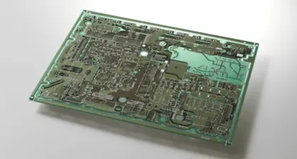
Printed circuit boards (PCBs) form the base of almost every electronic product, from smartphones and communication equipment to EVs, industrial systems, medical devices and data‑center servers. Wherever electricity flows, PCBs are essential.
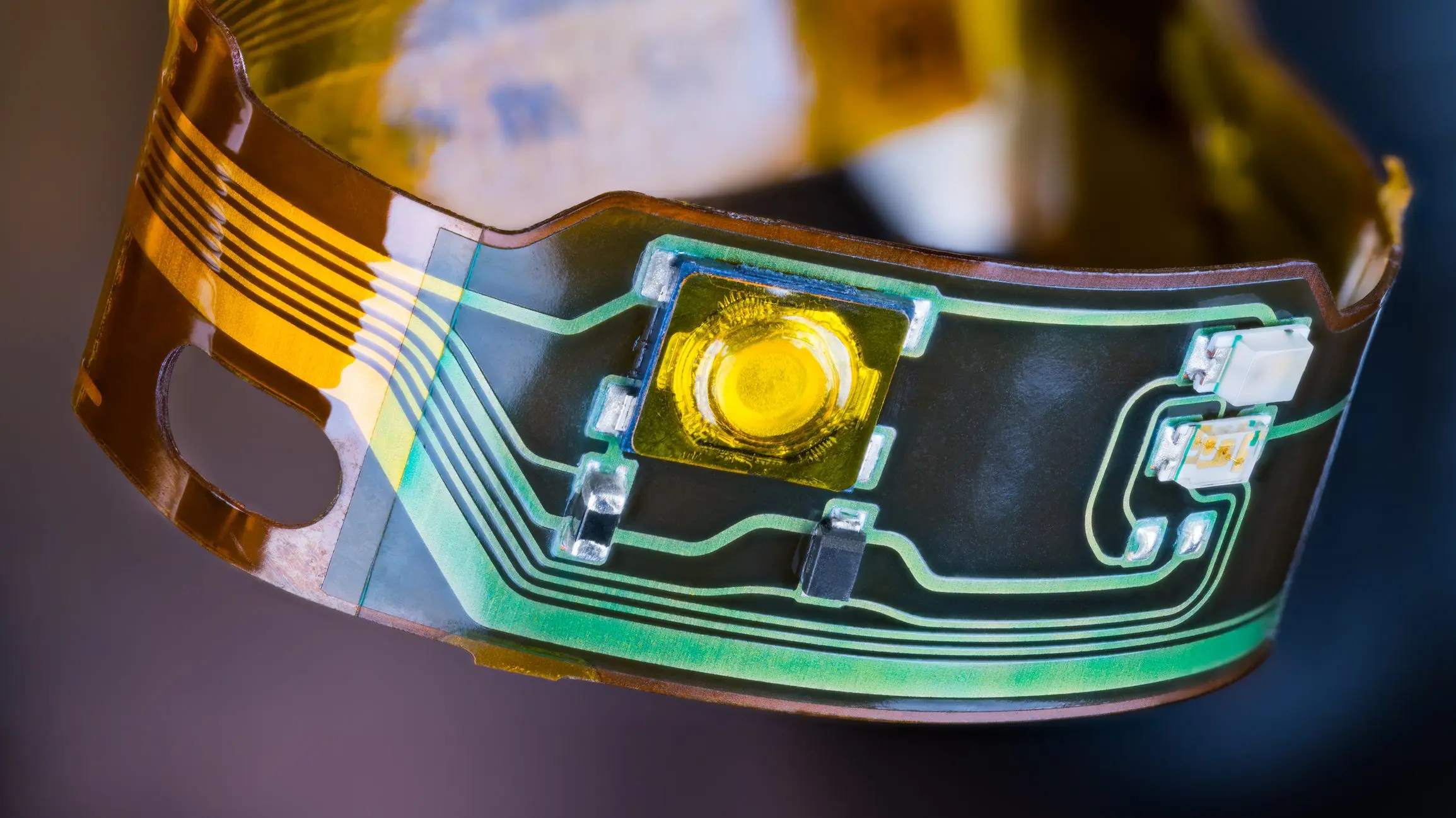
PCB technology creates precise electrical pathways that connect electronic components to each other. As devices become smaller and more functional, the wiring on these boards is now required to be finer than a human hair.
“By using multilayer boards and routing circuits in three dimensions, we can improve device performance and reduce electrical noise. This helps us achieve higher reliability in terms of mechanical strength, heat resistance and stable operation over a long period. At Shinko, our customers value us as a partner for our unique technologies, strong proposal capabilities and reliable manufacturing,” says Takagi.
Expanding PCB demand and the value of Japanese quality
In recent years, electronic devices have been improving performance while shipment volumes keep increasing. As a result, not only is demand for PCBs increasing, but the technical requirements for PCB technology are also becoming more diverse and more advanced.
Most electronic products are required to be smaller and lighter, while offering more functionality. PCBs are no exception. In addition to quality and reliability, they also need to become thinner, lighter and more compact and this requirement is growing stronger every year.
Shinko’s processing technologies are designed to meet exactly these needs. The company has supported many customers who want PCBs that are smaller, more densely packed and more functional than before.
“What supports our technology is not just high precision,” Takagi explains. “It is our advanced and flexible approach to processing. We can handle complex shapes and types of machining that are difficult with standard methods. This uniqueness is a major strength of Shinko’s technology.”
Three key points support Shinko’s advanced technical capabilities:
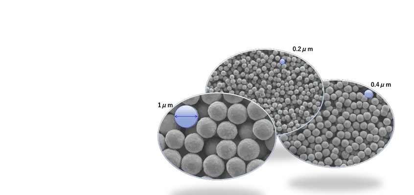
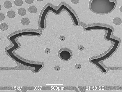
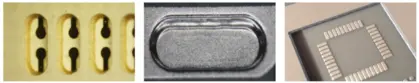
In PCB manufacturing, various types of holes must be created, including holes that carry electrical signals. These are usually made using drills or lasers. In addition to these standard methods, Shinko applies a sandblasting process (abrasive blasting) to hole formation and has successfully adapted this method for PCB mass production.
In this process, very fine abrasive particles, measured in micrometers, are blasted onto the material at high speed. This allows Shinko to create holes in shapes other than simple circles and to form “cavity” structures that give the board a three dimensional profile.
The process also produces smooth cut surfaces and can machine many small, high precision holes at the same time. It makes it possible to create micro holes that are difficult to achieve with conventional methods, helping the company respond to growing needs for miniaturization.
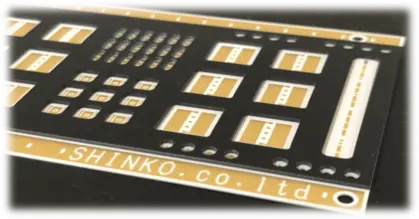
While standard PCBs are flat, Shinko can machine boards into “cavity PCBs” with three dimensional structures, such as steps or recesses in the board.
By using these height differences, designers can:
Cavity PCBs can also help reduce the number of molded plastic parts and simplify assembly steps, which can lower costs and improve reliability.
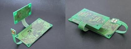
Shinko is also developing “semi flex PCBs” by applying its cavity processing technology. Normally, rigid PCBs are stiff and do not bend. However, by making certain areas thinner through cavity processing, those sections can flex without cracking or breaking when bent.
Using semi flex PCBs can reduce the number of parts such as connectors and wiring cables. This gives customers more freedom in product design and can also:
Semi flex PCBs are expected to be adopted in areas such as medical devices, in vehicle systems, measuring instruments and wearable devices.
Another strength of Shinko is its collaboration with Sumitomo Metal Mining, a company with strong expertise in materials. By using Sumitomo’s knowledge of material properties, Shinko can develop optimal processing methods. This joint work supports everything from process development to improved manufacturing capabilities and helps solve many kinds of technical challenges.
Advances in PCB technology do not only improve performance. They can also help reduce environmental impact.
As explained above, custom designs and made to order solutions that use advanced processing can combine or simplify production steps. This can lead to a reduction in the total amount of material used.
Looking ahead, there is also potential to introduce printed electronics into part of the PCB manufacturing process. Printed electronics use conductive inks to “print” circuits. If this approach is applied where appropriate, it could further reduce both material usage and the number of processing steps.
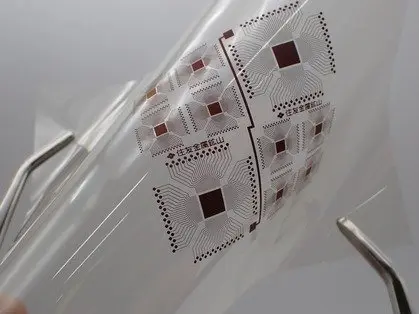
Today’s mainstream method for forming circuitry is as follows: a metal foil is laminated to the PCB surface, a photoresist is applied on top, and the unwanted metal is removed chemically using the photoresist as a mask. A photoresist is a light sensitive material used to selectively “keep or remove” metal according to the circuit design.
In contrast, printed electronics form circuits only where they are needed. This reduces material waste. It also removes the need for photoresist in those areas and can cut the number of process steps.
“We expect to see this technology introduced in some types of PCBs, especially for general purpose equipment and consumer appliances, in the not too distant future,” says Takagi.

PCB technology continues to advance, supporting products across a wide range of products, from smartphones to industrial robots.
If you are considering a new product development, pursuing size or power reductions, refining an existing product or reducing environmental impact, we encourage you to consult with X MINING.
Written by: X‑MINING Editorial Team
Ready to get started? Contact us to talk about your requirements.
Introducing Sumitomo Metal Mining’s material products,
which are the starting point for X-MINING innovation.