Article
閉じる
閉じる
Search
Ultra-Thin Copper Layer:
Thin and uniformed
copper layer of 0.1µm to 9µm
enables precise patterning
Folding endurance:
Low spring-back and high folding endurance for thinner devices.
Transparency:
Flat film-metal interface,
applicable for transparent materials
Flatness:
High insulation reliability due to flat film-metal interface.
*Note: Nominal values from our R&D shown above. Please show us your requirements, and let us discuss about detailed specifications.
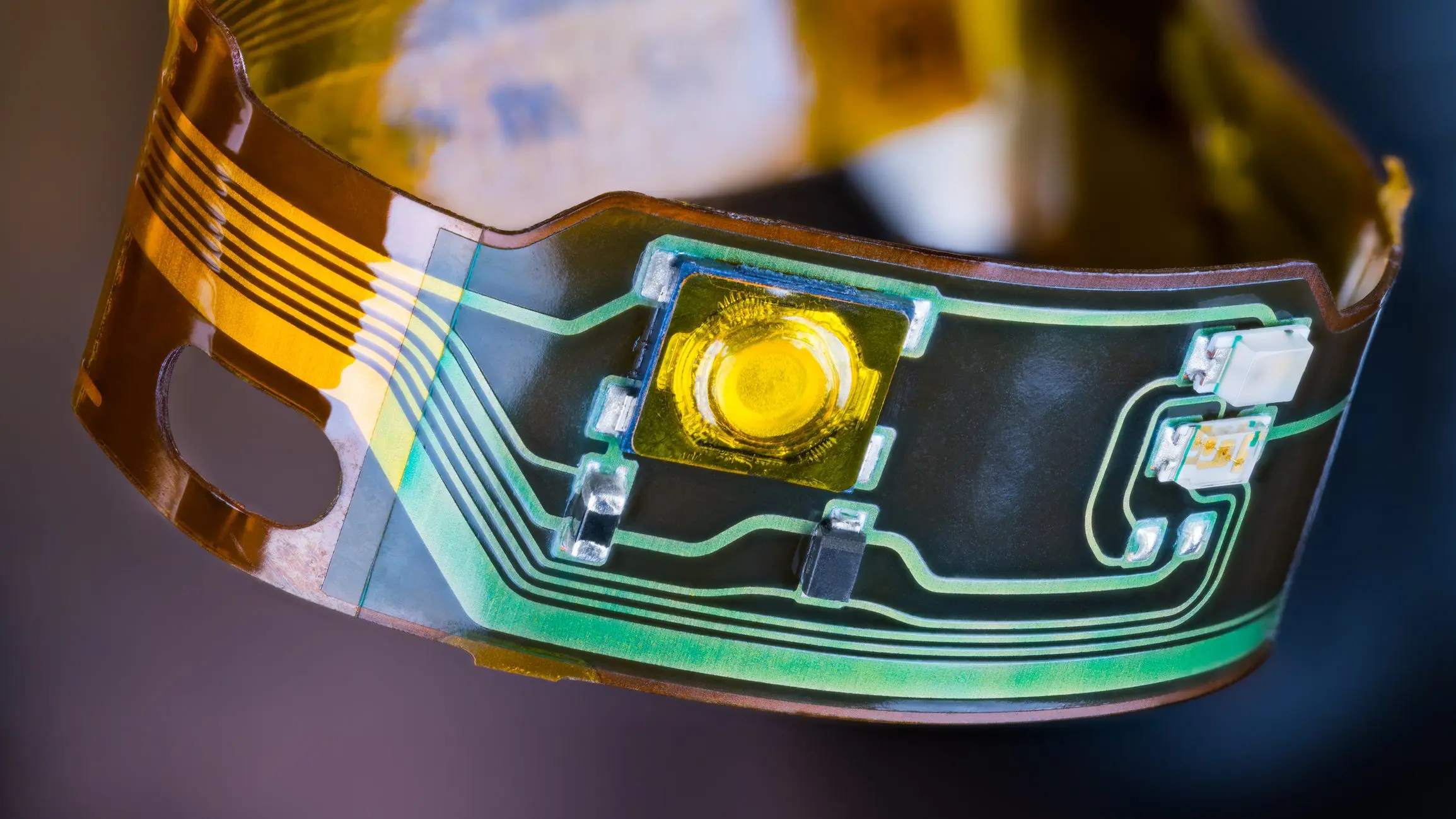
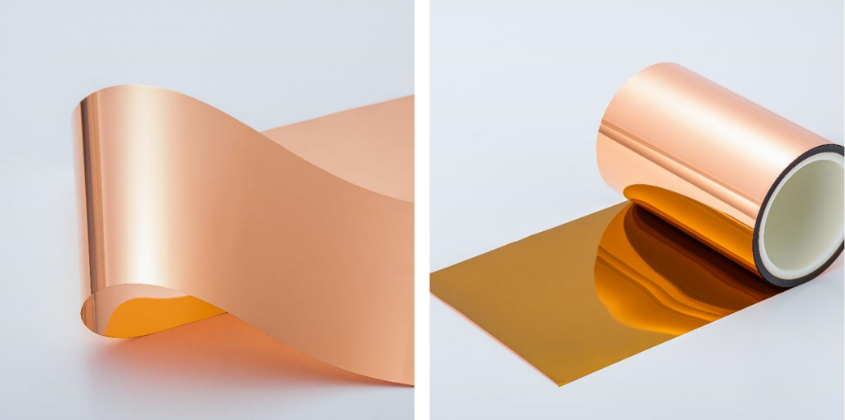
Sumitomo Metal Mining’s Copper Clad Laminate is a flexible substrate material with copper layer formed on various organic resin films such as polyimide or transparent films. The flat film-metal interface and thin, uniformed copper layer realizes precise patterning. Transparent FCCL, with copper layer formed on transparent films, can be processed into products such as transparent antennas and FPCs.
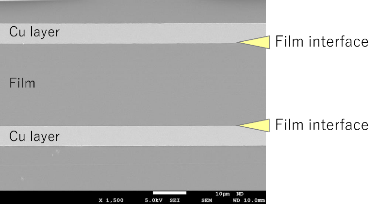
・The Flat film-metal and thin, uniformed copper layer enable to process high precision patterning.
・The copper layer thickness can be adjusted from 0.1µm to 9µm to suit for subtractive or semi-additive processes (SAP, MSAP).
・Capable to fabricate FCCL with various organic resin films.
・FCCL with 12.5µm thick polyimide film enables to process thin and highly integrated electronic devices.
・FCCL with transparent film without adhesive maintains the flat film surface and transparency even after patterning.
・Various transparent films such as PET film, Colorless PI film with heat-resistance or COP film with high transparency and low transmission loss can be applied, to suit for various applications such as transparent displays, transparent FPCs, transparent antennas or transparent heaters.
Metalized FCCL expected to replace for traditional FCCL with copper foils in applications required to be thin, light and flexible.
・Combination of various films and copper thickness can be selected.
・For Sumitomo Metal Mining’s Copper Clad Laminate , various organic resin films and copper layers with wanted thickness can be selected. Please show us your selection and wants.
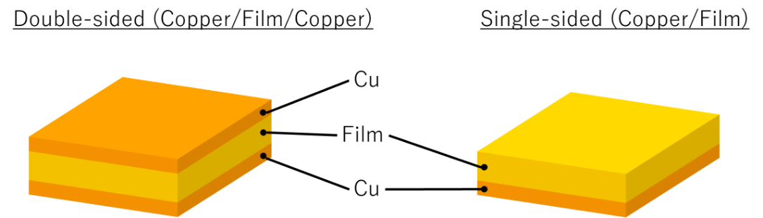
| Film | Copper layer | Shape |
|---|---|---|
| Polyimide film Transparent films, etc. |
Single-sided (copper/film) Double-sided (copper/film/copper) Standard thickness 0.3 μm, 2 μm, 8 μm (available down to 0.1μm as option, please contact us) |
Roll type, (for width or length, please contact us) |
For more details, please download for detailed product information, including specifications.
Click below to access.
S’PERFLEX
FCCL can be used as materials for patterning various electric circuits.
The thickness of the copper layer can be selected to match processing method. For example, copper layer of 0.1μm to 4μm for semi-additive process (SAP,MSAP), 6μm to 8μm for subtractive process and 2μm to 5μm for subtractive process with panel-plated through-hole.
Transparent FCCL applying transparent films can be used to fabricate transparent FPC without impairing visibility.
SMM FCCL adopts Roll to Roll process to suit mass production.
SMM FCCL can be a substitute for copper foil in parts to be thinner, lighter and more flexible.
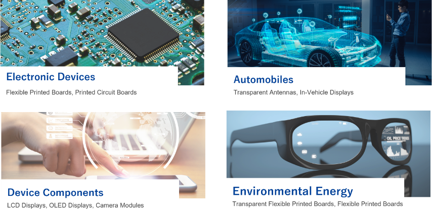
SMM FCCL is mainly used as material to fabricate substrates for mounting driver IC in LCDs and organic EL displays, and are used in TVs, monitors, mobile PC, smart phones, and tablets. In future, they are expected to be used in electronic paper and monitors inside automobiles.
Transparent FCCL applying transparent films can be used for transparent displays and transparent FPC, transparent antennae, and transparent heaters.
・Copper Clad Laminate (2-layer FCCL) without adhesive: Conventional CCL using adhesives may cause short circuits due to metal residue after precise patterning. In some cases, this issue had been solved using SMM 2-layer FCCL and succeeded in improving the reliability of driver IC circuits for LCD and OLED displays.
・Copper Clad Laminate (Transparent FCCL) using transparent films: Trade-off between transparency and conductivity to be cleared for fabrication of transparent antennas or FPCs. SMM 2-layer FCCL enables precise patterning with visibility by maintaining linearity of lines after processing. This can promote scope of new products such as transparent antennas, heaters, displays and so on.
ombining Sumitomo Metal Mining’s expertise with industry insights, X-MINING is here to innovate and solve challenges.
If you see potential, don’t hesitate to reach out with any questions you may have!
Introducing Sumitomo Metal Mining’s material products,
which are the starting point for X-MINING innovation.